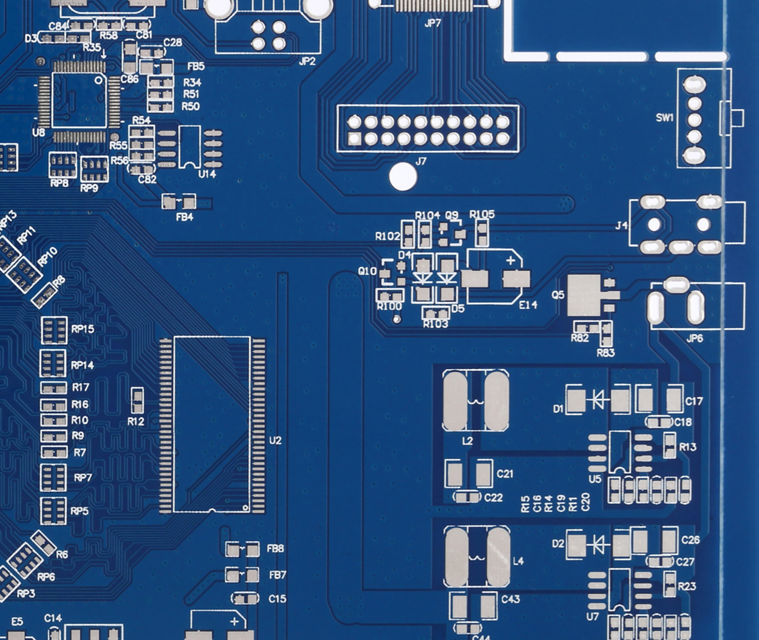
Stress screening refers to the application of acceleration techniques to add environmental stress to the product under the design strength limit, such as: burn in, temperature cycling, random vibration, power cycle And other methods, through accelerating the stress to make the latent defects of the product emerge [potential parts material defects, design defects, process defects, process defects], and eliminate the residual stress of electronics or machinery, as well as eliminate the stray capacitance between multilayer circuit boards, and remove and repair the products in the early infancy stage in the bathtub curve in advance, so that the products can preserve the products in the normal and declining stages of the bathtub curve through appropriate screening, In order to avoid the failure and unnecessary loss of the product when it is tested by environmental stress in the process of use, although the use of ESS stress screening will increase the cost and time, it has a significant effect on improving the product delivery yield and reducing the number of repair, but it will reduce the total cost, and the customer trust will also be improved. Generally, the stress screening methods for electronic parts include pre burning, temperature cycling At high temperature and low temperature, the stress screening method of PCB printed circuit board is temperature cycle. The stress screening for electronic cost is: power on pre burning, temperature cycle, random vibration. In addition, the stress screen itself is a process in the process stage, not a test. Screening is a 100% process for products.
The failure modes triggered by the temperature cycling test chamber or their effects on the products are as follows:
a. Make all kinds of micro cracks on the coating, material or thread head expand
b. Loosen the poorly bonded joint
c. Loosen the joints with improper screw connection or riveting
d. Loosen the press fitting joint with insufficient mechanical tension
e. Increase the contact resistance of poor quality solder joints or cause an open circuit
f. Particle and chemical pollution
g. Seal failure
h. Packaging issues, such as the connection of protective coatings
i. Transformer and coil short circuit or open circuit
j. Defective potentiometer
k. Poor connection of welding and fusion points
l. Cold welding contact
m. Open circuit and short circuit of multilayer board due to improper handling
n. Power transistor short circuit
o. Poor capacitors and transistors
p. Damage of dual integrated circuit
q. Cable box or cable that is almost short circuited due to damage or improper assembly
r. The material is broken, cracked and scored due to improper treatment etc.
s. Out of tolerance parts and materials
t. The resistor broke due to lack of synthetic rubber buffer coating
u. Hair crack occurs when the metal strip of the transistor is grounded
v. The mica insulating gasket is broken, resulting in a short circuit of the transistor
w. The metal sheet of the coordination coil is improperly fixed, resulting in irregular output
x. Two pole vacuum tube opens internally at low temperature
y. Coil indirect short circuit
z. Ungrounded connector
A1. component parameter drift
A2. improper installation of components
A3. Misuse of components
A4. Seal failure